
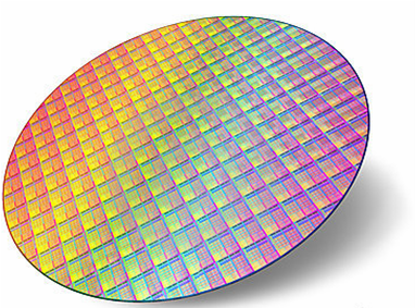
Wafer Backend Process
Product Experience– Wafer Level
Q3’2026 Ready
Bumping
- 8” & 12” Wafer
- Solder Bump
- Copper Pillar
- RDL
Q4’2025 Ready
Wafer Probing
- SiPh Wafer Level Test
- Automatic Fiber Alignment
Wafer Grinding
- 8” & 12” Silicon Wafer
- Non-bumped: Min 50um
- Bumped: Min 110um
- Auto Frame Mounting
Wafer AOI
- 2D & 3D Inspection
- Min Defect Size 1.56um
- Incoming and Post Dicing
Chip on Wafer
- +/-3um Accuracy
- Flux Dipping
- Laser Soldering
Laser Grooving
- Low K Wafer
- Groove Width 60um
Wafer Recon
- +/-30um Accuracy
- Hoop Ring/Gel Pak
- 6 sides AOI
- Min Defect Size 15um
Stealth Dicing
- SiPH Stealth Dicing
- Back Side Through Tape
- +/-3um Dicing Accuracy
- Wafer backgrinding process capability
- Wafer size:8inch, 12inch
- Final thickness: min. 50um
- Tolerance:±10um
|
|
- Wafer dicing saw process capability
- Provide different size vacuum chuck table
- DI water with CO2 and diamaflow to avoid ESD and contamination issue.
- Provide various dicing blade and optimal process solution according to different wafer material (Si, COMS, LiTaO3, glass, etc.)
|
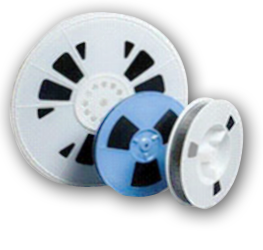
- Dice tape & Reel process capability
- Six side AOI (Missing bump, crack, chipping, contamination, etc.)
- UPH:12~14k
- Min. dice size:0.3*0.3mm
- Dice type: Si, SiGe, GaAs
|
|
Address:A part of Land Lot H, Quang Chau Industrial Park, Nenh Town, Viet Yen District, Bac Giang Province, Vietnam. TEL:+84-24-32045591
© Copyright 2020-2021 Shunyun technology ( Bac Giang, Vietnam) Limited. All Rights Reserved. | Best browse in 1024x768 pixel with IE 8.0 or above.